TEM Grid
Sample: A 200 mesh copper transmission electron microscope (TEM) grid.
Source: Organishe Chemie III, Ulm, Germany.
Science!
A transmission electron microscope is a way of investigating objects much smaller than a wavelength of light. The general principle is similar - use a beam of electrons that is trransmitted through a copper mesh, but is stopped by your objects under study. You can see things as small as single atoms with a good enough instrument.

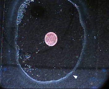
TEM Grid Back, 10x.

TEM Grid Back, 60x.

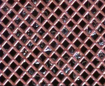
TEM Grid Back, 200x.

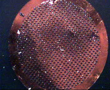
TEM Grid Front, 10x.

TEM Grid Front, 60x.
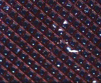
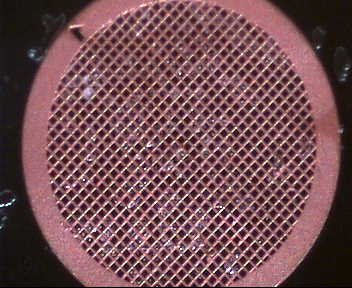
TEM Grid Front, 200x. Tiny holes! The diagonal across one of those squares is about a millimeter.

TEM Grid, 22,000x. These are nanoparticles of polyvinylcaprolactam (PVCL) and polyperfluorodecylmethacrylate (PPM). The large particles are mostly PVCL, and the small ones are PPM.

TEM Grid, 36,000x. I want one of these microscopes.
Source: Organishe Chemie III, Ulm, Germany.
Science!
A transmission electron microscope is a way of investigating objects much smaller than a wavelength of light. The general principle is similar - use a beam of electrons that is trransmitted through a copper mesh, but is stopped by your objects under study. You can see things as small as single atoms with a good enough instrument.
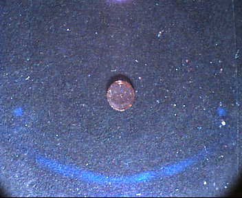
TEM Grid Back, 10x.
TEM Grid Back, 60x.
TEM Grid Back, 200x.
TEM Grid Front, 10x.
TEM Grid Front, 60x.

TEM Grid Front, 200x. Tiny holes! The diagonal across one of those squares is about a millimeter.

TEM Grid, 22,000x. These are nanoparticles of polyvinylcaprolactam (PVCL) and polyperfluorodecylmethacrylate (PPM). The large particles are mostly PVCL, and the small ones are PPM.

TEM Grid, 36,000x. I want one of these microscopes.
posted by Jacob at 12:12 PM
![]()

2 Comments:
Jacob - I realize that I could get a good estimate using your "1mm across the diagonal" figure, but counting those tiny squares didn't appeal. How big is the disk itself?
They're about three millimeters across, and wafer-thin. I just counted the number of holes across, since at 200x the field of view is about one millimeter.
I believe that these grids are "200 mesh," which means that (quantitatively) the holes are really more like .74 millimeters square, and the bars about .3 millimeters wide.
Post a Comment
<< Home